- 您现在的位置:买卖IC网 > Sheet目录1215 > EVDP610 (IXYS)BOARD EVALUATION IXDP610
�� �
�
�EVDP610�
�the� user� can� choose� between� three� different� PWM� base�
�periods� for� any� given� external� CLOCK� frequency.�
�ground.� Pin� 1� on� the� board� is� indicated� by� the� square�
�via.� This� provides� easy� access� for� outside� wires� or� a�
�wiring� harness� to� connect� to� another� board.�
�When� the� IXDP610� is� programmed� in� 8-bit� mode,� the�
�PWM� base� period� is� equal� to� 256� PWM� clock� cycles.�
�In� 7-bit� mode� the� PWM� base� period� is� equal� to� 128�
�PWM� clock� cycles.� A� PWM� clock� cycle� is� equal� to�
�one� external� CLOCK� period� when� the� clock� is� divided�
�by� one.� The� following� formulas� can� be� used� to� deter-�
�mine� the� PWM� base� period:�
�If� 7-bit� resolution� and� clock� divide� by� 1� ->� PWM� base�
�period� =� CLOCK� period� x� 128�
�If� 8-bit� resolution� and� clock� divide� by� 1� ->� PWM� base�
�period� =� CLOCK� period� x� 256�
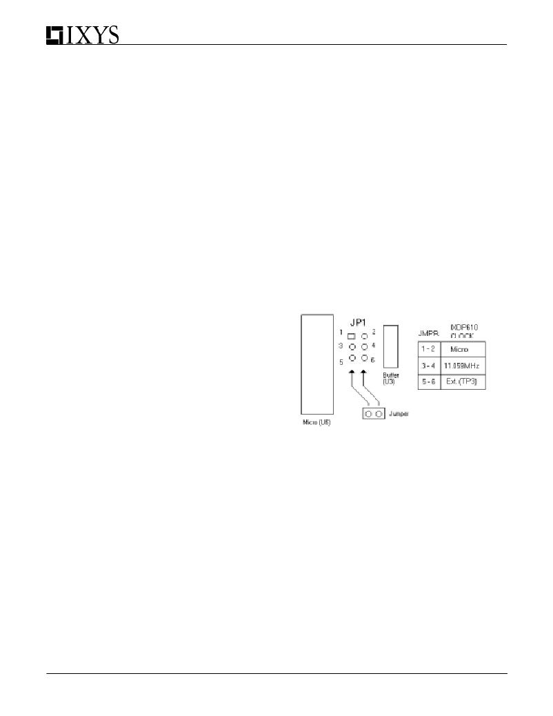
�2.3� Input� Clock� Selection� and� Jumper� Settings�
�The� evaluation� board� has� 3� jumper� settings� (labeled� JP1�
�on� the� board)� that� allow� the� user� to� switch� between� three�
�input� clock� selections:�
�1)� Using� the� microprocessor� to� clock� the� IXDP610.�
�2)� Using� the� on-board� 11.059� MHz� to� clock� the�
�IXDP610.�
�3)� Hooking� up� an� external� clock� signal.� For� this�
�either� wire� the� clock� signal� to� the� jumper� itself�
�or� the� user� can� use� the� TP3� via.�
�If� 7-bit� resolution� and� clock� divide� by� 2� ->� PWM� base�
�period� =� CLOCK� period� x� 256�
�If� 8-bit� resolution� and� clock� divide� by� 2� ->� PWM� base�
�period� =� CLOCK� period� x� 512�
�2.2.5� Stop�
�This� bit� in� the� control� latch� of� the� IXDP610� enables� and�
�disables� the� outputs.� When� enabled,� the� outputs� will�
�not� be� re-enabled� until� the� start� of� the� PWM� period.�
�2.2.6� ODIS� :� Output� Disable�
�Referred� to� as� the� OUPUT� DISABLE� pin,� this� pin� on� the�
�IXDP610� is� connected� to� a� jumper� on� the� board� (labeled�
�JP2),� which� is� tied� to� a� pull-up� resistor� before� the�
�jumper� is� installed.� Installing� a� jumper� onto� these� pins�
�asserts� the� ODIS� pin� (ties� the� pull-up� to� ground� putting�
�a� low� signal� onto� ODIS).� Asserting� ODIS,� or� the�
�OUTPUT� DISABLE� pin,� on� the� IXDP610� forces� the�
�complementary� outputs� to� be� immediately� disabled�
�(forced� low).� These� outputs� will� remain� low� as� long� as�
�this� input� is� asserted,� and� for� the� duration� of� the� PWM�
�cycle� in� which� OUTPUT� DISABLE� goes� from� low� to�
�high;� i.e.,� the� complementary� outputs� are� not� re-�
�enabled� until� the� beginning� of� the� next� PWM� cycle,� and�
�then� only� if� the� both� ODIS� and� Stop� are� not� enabled.�
�*For� more� information� on� technical� specifications� of� the�
�IXDP610� IC,� please� see� the� IXDP610� documentation�
�which� can� be� downloaded� from� the� IXYS� website�
�(www.ixys.com).�
�2.2� Outputs�
�The� IXDP610� chip,� labeled� U1� on� the� evaluation� board,�
�and� its� complementing� outputs� (labeled� TP1� and� TP2)�
�can� be� accessed� either� with� the� black� and� white�
�terminals� provided� or� by� J4,� which� accommodates� a�
�four� pin� header.� Pin� one� and� three� on� the� header� are�
�the� output� signals� and� pins� 2� and� 4� are� connected� to�
�3�
�Figure� 5� shows� the� placement� of� the� jumper� for� each�
�setting.� Factory� default� is� the� middle� setting,� clocking�
�the� IXDP610� with� the� on-board� 11.059MHz� oscillator.�
�Figure� 5:� Placement� of� Jumper� for� IXDP610�
�Clock� Selection�
�2.3.1� Using� the� Microprocessor� as� the� Input� Clock�
�The� microprocessor� on� the� evaluation� board� can� be� used�
�as� the� clock� signal� into� the� IXDP610.� This� clock� can�
�provide� output� frequencies� of� 1� –� 50� Hz� on� the� IXDP610�
�chip.� Due� to� interrupt� latency� this� is� as� fast� as� the�
�microprocessor� can� clock� the� IXDP610� and� there� is� a� +/-�
�3%� frequency� error� associated� with� this� arrangement.�
�2.3.2� Using� the� 11.059� MHz� as� the� Input� Clock�
�This� is� set� as� the� factory� default;� it� allows� the� same� on-�
�board� oscillator� that� clocks� the� microprocessor� to� clock�
�the� IXDP610.�
�2.3.3� Using� an� External� Clock� Signal�
�Allowing� the� user� to� hook� up� an� external� clock� signal�
�allows� any� input� clock� (up� to� 50� MHz)� to� be� used� as�
�input� to� the� IXDP610.� This� results� in� output� frequencies�
�发布紧急采购,3分钟左右您将得到回复。
相关PDF资料
EYP-2MT098B
THERMAL CUTOFF 98C 2A/50VDC TAB
EZ3-A230XF1
SURGE ARRESTER 230V GASTUBE 3PIN
EZJ-Z1V39010
VARISTOR MULTILAYER 39V 0603
EZN-4100LCMUS-2
KEYBOARD EZCLEAN 83 KEYS USB
F0402G0R20FNTR
FUSE 0.20A 32V FAST THIN 0402
F1206A2R00FWTR\500
FUSE 2.00A 32V FAST THIN 1206
F1206B1R50FWTR
FUSE 1.50A 63V FAST THIN 1206
F200-003-R
CARD IEEE1394 FIREWIRE PCI
相关代理商/技术参数
EVDS430SI
功能描述:电源管理IC开发工具 30A Ultra Fast MOSFET/IGBT Driver RoHS:否 制造商:Maxim Integrated 产品:Evaluation Kits 类型:Battery Management 工具用于评估:MAX17710GB 输入电压: 输出电压:1.8 V
EVDXXXX
制造商:未知厂家 制造商全称:未知厂家 功能描述:MILITARY QUALITY REMOVABLE CONTACT, SUBMINIATURE-D CONNECTORS
EVE2-29A-BLM-TPN
功能描述:DISPLAY LCD TFT TOUCH RES 2.9" E 制造商:matrix orbital 系列:- 零件状态:在售 显示类型:TFT - 彩色 显示模式:可传导的 触摸屏:- 屏幕对角线尺寸:2.9"(73.66mm) 可视范围:72.10mm 宽 x 26.10mm 高 背光:- 点像素:320 x 102 接口:SPI 图形颜色:红色,绿色,蓝色(RGB) 背景颜色:黑色 点尺寸:- 点间距:- 标准包装:1
EVE2-35A-BLM-TPN
功能描述:DISPLAY LCD TFT 3.5" EVE 制造商:matrix orbital 系列:- 零件状态:在售 显示类型:TFT - 彩色 显示模式:可传导的 触摸屏:- 屏幕对角线尺寸:3.5"(88.90mm) 可视范围:73.10mm 宽 x 55.50mm 高 背光:- 点像素:320 x 240 接口:SPI 图形颜色:红色,绿色,蓝色(RGB) 背景颜色:黑色 点尺寸:- 点间距:- 标准包装:1
EVE2-35A-BLM-TPR
功能描述:DISPLAY LCD TFT TOUCH RES 3.5" E 制造商:matrix orbital 系列:- 零件状态:在售 显示类型:TFT - 彩色 显示模式:可传导的 触摸屏:电阻 屏幕对角线尺寸:3.5"(88.90mm) 可视范围:72.28mm 宽 x 54.76mm 高 背光:- 点像素:320 x 240 接口:SPI 图形颜色:红色,绿色,蓝色(RGB) 背景颜色:黑色 点尺寸:- 点间距:- 标准包装:1
EVE2-38A-BLH-TPR
功能描述:DISPLAY LCD TFT TOUCH RES 3.8" E 制造商:matrix orbital 系列:- 零件状态:在售 显示类型:TFT - 彩色 显示模式:可传导的 触摸屏:电阻 屏幕对角线尺寸:3.8"(96.52mm) 可视范围:96.84mm 宽 x 25.10mm 高 背光:- 点像素:480 x 116 接口:SPI 图形颜色:红色,绿色,蓝色(RGB) 背景颜色:黑色 点尺寸:- 点间距:- 标准包装:1
EVE2-43A-BLM-TPN
功能描述:DISPLAY LCD TFT 4.3" EVE 制造商:matrix orbital 系列:- 零件状态:在售 显示类型:TFT - 彩色 显示模式:可传导的 触摸屏:- 屏幕对角线尺寸:4.3"(109.22mm) 可视范围:98.70mm 宽 x 57.50mm 高 背光:- 点像素:480 x 272 接口:SPI 图形颜色:红色,绿色,蓝色(RGB) 背景颜色:黑色 点尺寸:- 点间距:- 标准包装:1
EVE2-43A-BLM-TPR
功能描述:DISPLAY LCD TFT TOUCH RES 4.3" E 制造商:matrix orbital 系列:- 零件状态:在售 显示类型:TFT - 彩色 显示模式:可传导的 触摸屏:电阻 屏幕对角线尺寸:4.3"(109.22mm) 可视范围:97.04mm 宽 x 55.85mm 高 背光:- 点像素:480 x 272 接口:SPI 图形颜色:红色,绿色,蓝色(RGB) 背景颜色:黑色 点尺寸:- 点间距:- 标准包装:1